PCB Design
PCB Design
- Width of the PCB traces should be 50% of the pitch to avoid short circuits
- Make PCB traces wider than flex traces to allow solder to flow and fillets to form
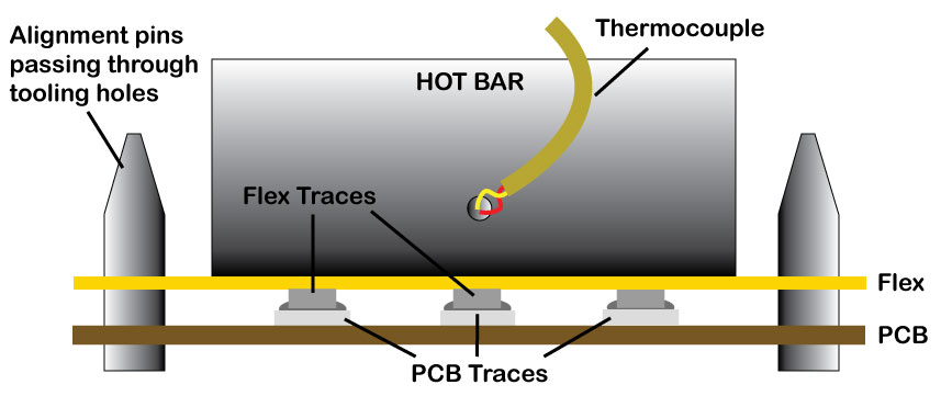
- Tooling holes in PCB and Flex allow easy alignment of traces
- Provide room for thermode to overhang both ends of pad area by 0.040”(1mm)
PROBLEM
Differences in heat sinking from pad to pad can cause uneven heating:
Unequal trace area and plated through holes act as a heat sink, causing uneven heat distribution.

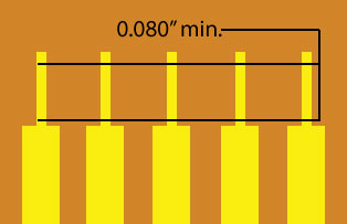
SOLUTION
Equal trace sizes (mass) leads to equal heating and better solder joint quality. Minimum .08" wide solder area is recommended.